|
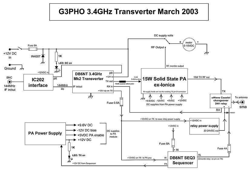
3.4GHz Transverter - page 5 The 15 watt system |
| To construct this 15 watt output transverter required several extra modules such as power supplies and an interface unit for the IC202S I.F or "prime mover". The block diagram below shows the basic system. A full size version of this can be found in the downloadable PDF document describing this transverter. All circuit diagrams of power supplies, etc, are also provided in the same document. |
|
|
|
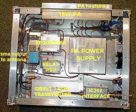
The photo above shows the modules that make up the block diagram. The 144MHz IF feeds(via the BNC socket in the lower right corner of the photo) the IC202 interface module, which grounds the PTT feedthrough on the DB6NT transverter when the IC202S is put in the Transmit mode. The Relay power supply is for the microwave coaxial changeover relay shown in blue near the sma output connector. The PA power supply module provides all the voltages required by the 15W PA and is switched on for TX only by the Sequencer, which is, in turn, switched on by the "+12V on TX" output from the DB6NT transverter module. |
|
|
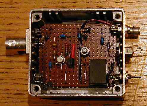 The
IC202S interface was built on perforated board (Veroboard)
using the copper strips on the underside to complete the electrical
circuitry. 144MHz I.F is applied to the BNC connector on the left
and the 144MHz RF passes on to the DB6NT module via the sma socket
on the upper right. The uppermost feedthrough capacitor is connected
to the PTT feedthrough on the DB6NT module, while the lower feedthrough
receives the +12DC supply for this unit. The relay, lower right,
keys the DB6NT transverter from receive to transmit when the PTT
switch on the IC202 microphone is pressed. The whole module is housed
in a small diecast box for efficient RF shielding purposes.
The
IC202S interface was built on perforated board (Veroboard)
using the copper strips on the underside to complete the electrical
circuitry. 144MHz I.F is applied to the BNC connector on the left
and the 144MHz RF passes on to the DB6NT module via the sma socket
on the upper right. The uppermost feedthrough capacitor is connected
to the PTT feedthrough on the DB6NT module, while the lower feedthrough
receives the +12DC supply for this unit. The relay, lower right,
keys the DB6NT transverter from receive to transmit when the PTT
switch on the IC202 microphone is pressed. The whole module is housed
in a small diecast box for efficient RF shielding purposes. | NEXT PAGE |